× CLOSE
ELECTRONICS DEPARTMENT
Electronics Department
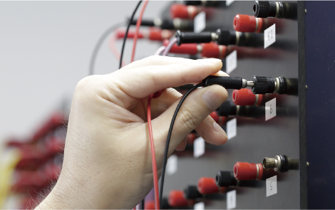
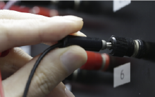
Exhaustive quality control
and the concentration of advanced technologies
Craftsmanship based on the concentration of advanced
technology with a steady eye developed through long experience
Flat Electronics is constantly improving its products to provide the highest possible quality, in order to support and advance today’s technology.
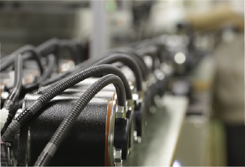
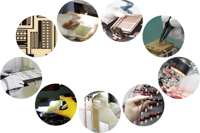
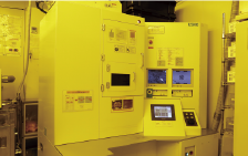
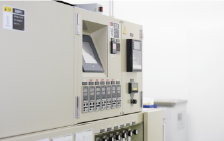
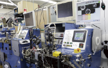
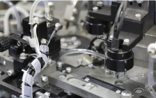
Process
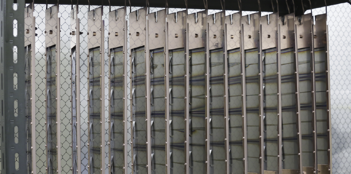
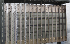
Manufacturing Processes
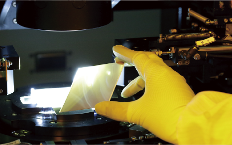
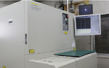
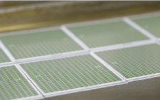
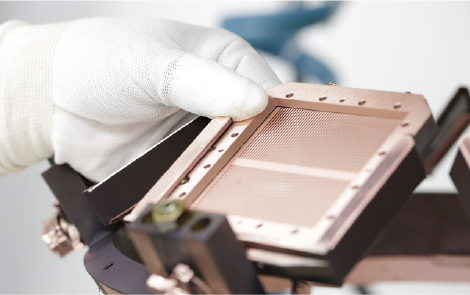
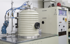
01Sputtering
Sputtering forms resistors and electrodes with high adhesion.
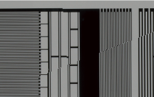
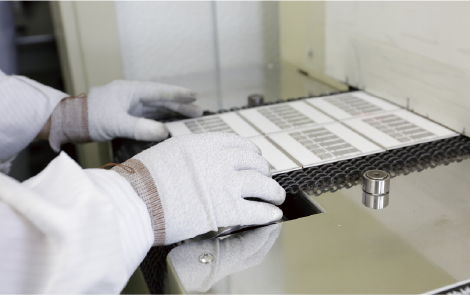
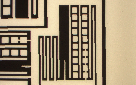
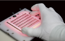
02Photo lithography
Photo lithography forms resistance patterns with line widths of 10μ or less.
03Annealing
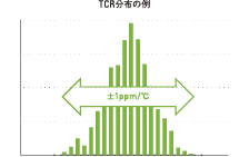
Annealing stabilizes resistive films, to achieve temperature coefficient of 1ppm/°C.
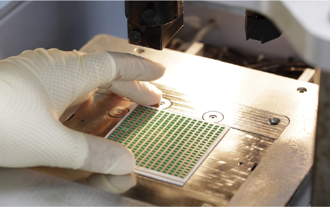
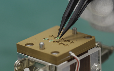
04Laser trimming
Laser trimming uses a laser to cut resistance patterns, to achieve resistance value precision of 0.01%.
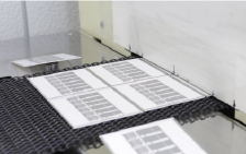
05Screen printing
Screen printing prints an epoxy-type protective layer to maintain the moisture resistance of resistors.
06Vapor deposition
Vapor deposition forms side-face electrodes on chip components.
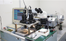
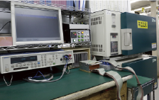
07TCR inspection
TCR inspection precisely measures the temperature properties of resistances.
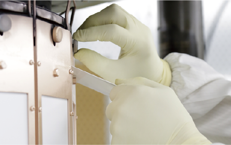
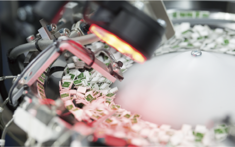
08Inspection taping
This process automatically inspects resistance values and appearance, and packages components.
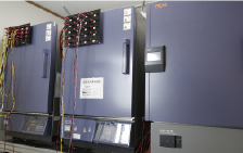
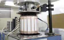
09Reliability testing
Test conditions vary temperature, humidity, atmospheric pressure, and input power, to ensure the reliability of resistances in the market.